// TOM'S HARDWARE US — HARDWARE & GADGET
Micron's next-generation 3D NAND to double bit density with over 400 layers, offering extreme performance
But can it make client SSDs cheaper and more capacious?
When you purchase through links on our site, we may earn an affiliate commission. Here’s how it works.
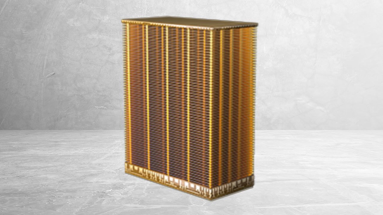
Micron's next-generation 3D NAND, which will enter mass production in 2H 2027, is set to offer three significant advantages: it will double storage density, increase I/O performance by 50% compared to the company's current-generation NAND memory, and decrease power consumption, the company revealed at an event this week. To achieve these aggressive goals, Micron plans to take a page from YMTC's book and adopt wafer-on-wafer bonding. Meanwhile, Micron is also developing new materials and denser memory cell architectures to extend 3D NAND scaling beyond G11.
"We had mentioned we will bring in wafer-on-wafer bonding technology at the right time when it’s cost-effective, and it brings in capability that is important for the product specs at the time, and this is the right timing for that technology," said Scott DeBoer, president and chief technology and products officer at Micron, during the company's event this week. "So this G11 technology is the world's most advanced NAND. It will ramp in the second half of next year, [and] it is based on wafer-on-wafer bonding technology."
Micron's G11 3D NAND represents a substantial advancement over its current G9 (N160) generation. The company expects the new memory to achieve approximately twice the bit density of G9 (3D TLC 21 Gb/mm2 => 3D TLC 42 Gb/mm2?), which means a dramatic increase compared to Kioxia's BiCS10 or Samsung's V10; increase I/O speeds by up to 50% (3,600 MT/s => 5,400 MT/s?); and reduce data transfer energy consumption per bit by more than 25%.
These improvements should benefit both conventional high-capacity SSDs for client and data center applications and emerging AI-oriented storage devices, which require greater bandwidth and energy efficiency.
One of the key changes introduced with G11 is wafer-on-wafer bonding, which enables Micron to manufacture different parts of its NAND device on separate wafers using different process technologies — a new 3D NAND node to build a NAND array and a logic fabrication process to make peripheral circuits and I/O — and subsequently bond them together. The company has used CMOS-under-array architectures for several generations. Still, wafer bonding provides additional flexibility to optimize memory arrays and peripheral logic independently, which means more capacity and performance if all goes as planned.
Another important innovation is the transition to more than 400 NAND layers. Micron has not disclosed the exact number of active wordline layers or the number of memory decks used by G11, but the company says the technology will feature an industry-leading memory cell pitch, which suggests that its density improvements will come from both additional layers and smaller cell dimensions.
Micron expects to disclose more technical details about G11 in 2027, closer to the start of high-volume manufacturing in the second half of next year.
Get Tom's Hardware's best news and in-depth reviews, straight to your inbox.