// NATURE NEWS — SPAZIO & SCIENZA
Low-power 2D CFETs using single-crystal high-κ dielectrics
Nature
(2026) Cite this article
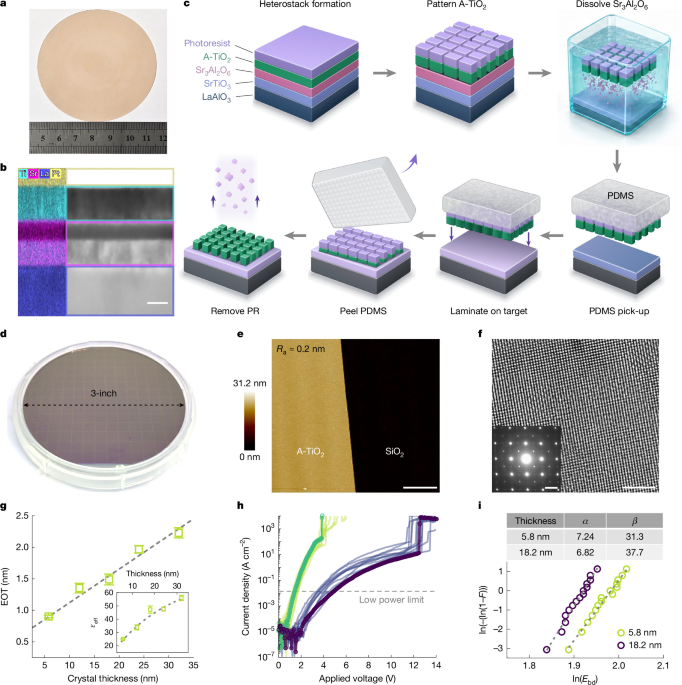
Aggressive scaling in silicon electronics—although essential for improving power, performance, area and cost—faces increasing challenges in further reducing power consumption due to electrostatic and leakage constraints1,2. Achieving efficient operation at low supply voltages therefore requires new materials and gate-stack engineering strategies. Two-dimensional (2D) semiconductors offer intrinsic advantages because their atomic thickness affords excellent gate control, and their sizable bandgaps suppress off-state current. However, a major obstacle is the imperfect interface between 2D channels and gate dielectrics, which degrades subthreshold swing, hysteresis and bias-temperature instability3. Here we demonstrate that a wafer-scale, transferable, single-crystal anatase titanium dioxide dielectric can be van der Waals integrated with 2D transition metal dichalcogenides. The obtained pristine 2D-dielectric interface enables subthreshold swing close to the thermal limit, record-low hysteresis and well-matched transfer characteristics for both n- and p-type enhancement-mode field-effect transistors. Building on this, we demonstrate complementary field-effect transistors, whose inverters achieve high voltage gain and large noise margins with subpicowatt static power consumption. These results highlight the promise of 2D semiconductors for ultra-low-power operation.
Modern silicon transistors continue to improve with technological advancement. However, as scaling progresses, power efficiency has emerged as a critical constraint, especially for ultra-low-energy applications such as wearable electronics, implantable medical devices, Internet of Things (IoT) nodes, edge AI processors and distributed sensor networks. To achieve substantial power reductions, device operation at reduced supply voltages has been explored extensively4,5. Nevertheless, silicon’s relatively small bandgap inherently increases leakage, while maintaining strong electrostatic control at scaled dimensions remains challenging6. A recent simulation study that compares silicon transistors with planar 2D field-effect transistors (FETs) from 16 nm to 1 nm technology nodes highlighted the low-power potential of 2D FET-based circuits7. These observations motivate the investigation of 2D semiconductors for low-power operation8,9,10,11,12.
The sizable bandgaps of 2D semiconductors suppress off-state current, while their atomically thin van der Waals (vdW) structure enables excellent gate control, making them well suited for energy-efficient operation. Proof-of-concept inverters assembled from n- and p-type 2D semiconductors—including MoS2-WSe2 (refs. 13,14,15), MoS2-MoTe2 (ref. 16) and pseudo-complementary metal–oxide–semiconductor (CMOS) based on single transition metal dichalcogenides (TMD)17—have demonstrated low-voltage and subthreshold operation with reduced static power consumption (Extended Data Table 1). However, these demonstrations rely on non-scalable approaches, such as mechanically exfoliated flakes or lateral assembly of dissimilar materials and devices. Their voltage gains are also limited (Extended Data Table 1), primarily because of asymmetric n-channel FET (n-FET) and p-channel FET (p-FET) transfer characteristics. One major source of this asymmetry is the gate stack: an imperfect 2D/high-κ interface degrades subthreshold swing, whereas unintentional dielectric-induced doping shifts the threshold voltage (Vth), impairing inverter performance. Most critically, WSe2-based p-FETs often have pronounced bipolar transfer characteristics, which are incompatible with robust CMOS operation and integration. High-permittivity, crystalline dielectric or buffer layers have been used to improve gate controllability by increasing gate capacitance and suppressing defect-induced degradation18,19,20. Clean vdW integration of gate dielectrics with 2D semiconductors also minimizes interfacial traps caused by