// TOM'S HARDWARE US — HARDWARE & GADGET
Mad scientist makes LEDs in his backyard — semiconductor wizard who made his own RAM turns his attention to using bathroom eBay laser to etch sapphire wafers
When you purchase through links on our site, we may earn an affiliate commission. Here’s how it works.
The Dr. Semiconductor YouTube channel only has a few videos, but the man is quickly making a name for himself. He's built a semiconductor cleanroom in his backyard and made his own RAM cells there. Matthew Hartensveld (his real name) needs to figure out a way to package (cut and write) the RAM cells, so he figure he might as well use the opportunity to make some free-range, homemade LEDs while he was at it. This latest adventure is part of his open-source Semiconductor.DIY project.
The entire video is fascinating and information-dense, so we suggest you watch it to get the complete picture. Hartensveld started off with gallium nitride atop a sapphire wafer, that he proceeded to break into shards and clean with a solution including deionized water, acetone, and isopropyl. The primary goal was to etch the top layer of the material in order to define pattern contacts. Chlorine gas would be the obvious answer as that's what's used industrially, but it'd be more than a little hazardous in this setting.
The scientist turned his attention to a household item that makes every nerd happy: lasers. He ordered a powerful one from eBay, and moved it into his bathroom so his dog wouldn't look into it. Hartensveld quickly came across the problem that there was basically no information online about using said laser, and after a few attempts he managed to etch some scribbles on the wafer, and then actual patterns. After this, he test-drove the "LED" shard by smooshing some indium on it and using a 9 V battery, and lo and behold, there was blue light.
Doing so left a deposit of metallic gallium atop the pattern, so he came up with a solution to clean that up to leave the etched parts clearly exposed. Using a vacuum chamber with a two-stage pump that sucked out 99.999999% of the air out, he deposited a nickel/silver layer for the positive contact, then a titanium/silver for the N-contact and top metal, using argon plasma as the top gas. Even still, he later regretted not letting the chamber run for a while longer to draw out yet more air, to reduce residual gas.
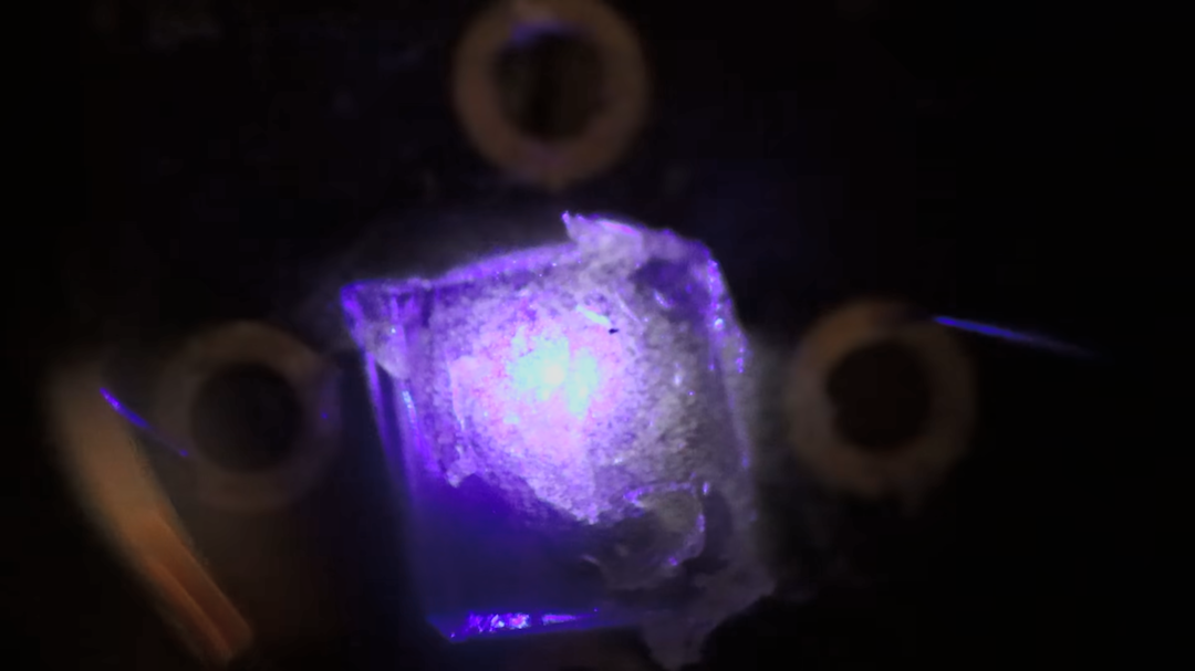
At this point, Hartensveld had a fully working blue LED, though still in a wafer. That's right, blue, the color of LED that was a mystery for decades until a dedicated Japanese engineer figured it out. At any rate, the time came to package these LEDs, meaning cut them out of the wafer, and add physical connections. A table saw with very thin blades didn't really worked out, so in pure scientist fashion, Hartensveld turned once again to the laser, focusing it at a specific point to melt away the sapphire substrate. After an adjustment to make this a multi-passs process, he finally had a full cut.
The madlad still needed to add wire connectors, and after evaluating a few options, settled on indium bumps, the same method and material used in digital cameras. Last but not least, since he already had a blue LED on hand, he added a layer of cerium-doped yttrium aluminum garnet (just bought off Alibaba) to add a yellow filter to end up with an ugly but functional white LED.
Follow Tom's Hardware on Google News, or add us as a preferred source, to get our latest news, analysis, & reviews in your feeds.
Get Tom's Hardware's best news and in-depth reviews, straight to your inbox.
Bruno Ferreira is a contributing writer for Tom's Hardware. He has decades of experience with PC hardware and assorted sundries, alongside a career as a developer. He's obsessed with detail and has a tendency to ramble on the topics he loves. When not doing that, he's usually playing games, or at live music shows and festivals.