// HACKER NEWS — CYBERSECURITY
Samsung Debuts zHBM Prototype, Stacking Memory Directly on AI Accelerators
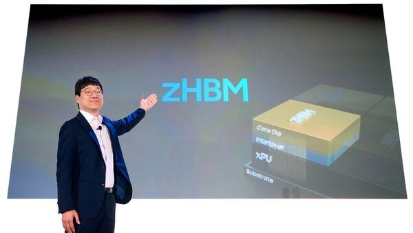
Samsung Electronics unveiled next-generation 3D memory technologies, including z-axis High Bandwidth Memory (zHBM) and zNAND-O, as the company seeks to strengthen its position in the rapidly growing artificial intelligence market.
Samsung on Aug. 5 showcased mockups of zHBM and zNAND-O for the first time at the Future of Memory and Storage (FMS) 2026 conference in California. During a keynote presentation on Aug. 4 local time, the company also outlined its vision for maximizing performance and power efficiency in high-performance computing (HPC) and AI systems through the use of zHBM, zNAND-O and other advanced memory technologies.
zHBM Delivers Up to Eight Times Higher Performance Through New Architecture
zHBM is a next-generation architecture that vertically stacks HBM on top of AI accelerators, or xPUs, along the z-axis. The design minimizes the distance data must travel between memory and AI processors, improving bandwidth and power efficiency while supporting the ultra-high-speed data processing required for training and inference of large-scale AI models.
Conventional architectures place HBM around the AI accelerator. Samsung said that approach faces limitations in meeting the performance requirements of next-generation HPC and AI infrastructure.
According to the company, zHBM can deliver up to eight times the data-processing performance of eighth-generation High Bandwidth Memory (HBM5) while improving performance per watt by a factor of three. Thermal resistance is reduced by more than half, enhancing both system stability and energy efficiency.
Samsung described zHBM as a customizable family of 3D memory products. The architecture allows customers to add semiconductor intellectual property (IP) blocks to an interlayer positioned between the memory and AI accelerator. These blocks can be tailored to expand memory capacity or optimize accelerator performance for specific workloads.
The company said it plans to work closely with customers to co-optimize AI processors and memory systems and maximize the performance potential of zHBM.
Samsung Reveals HBM-Like zNAND-O and 400-Plus-Layer V10 BV-NAND
Samsung also introduced zNAND-O, a next-generation high-performance NAND flash family currently under development. The technology combines Samsung's vertical V-NAND stacking architecture with Through-Silicon Via (TSV) technology. TSVs are used in HBM to electrically and physically connect vertically stacked DRAM dies. Samsung's zNAND-O adopts a structure similar to High Bandwidth Flash (HBF), which is being developed by SK Hynix and Sandisk.