// TOM'S HARDWARE US — HARDWARE & GADGET
Intel patent embeds MicroLEDs in chip packaging — technology may enable embedded optical interconnects through TGVs
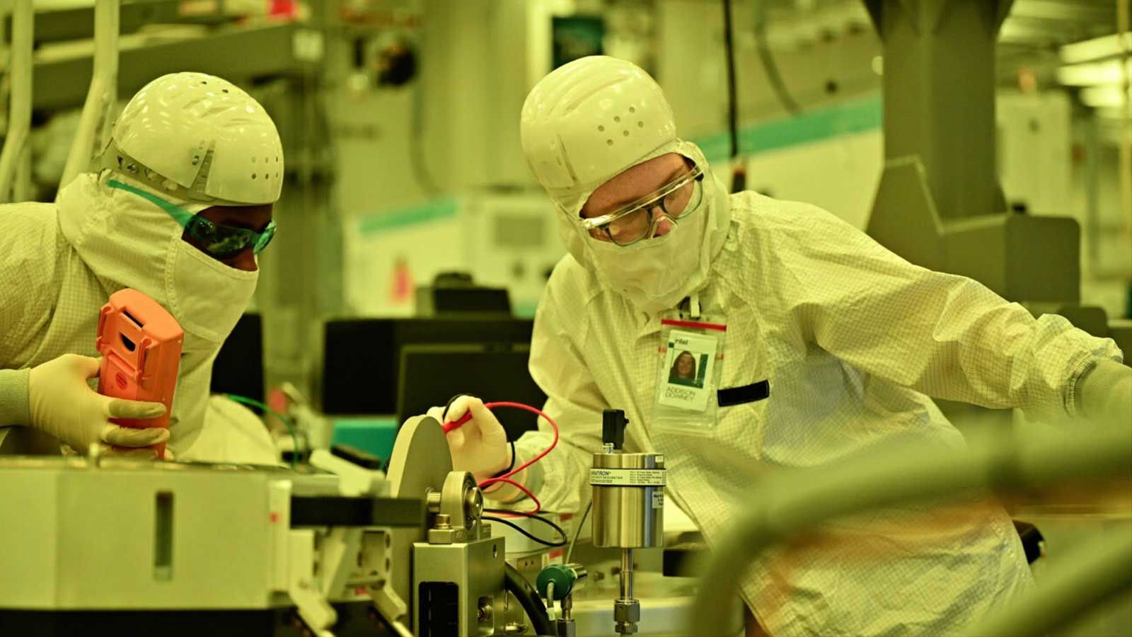
This follows over a decade of Intel investment in glass substrate technology.
When you purchase through links on our site, we may earn an affiliate commission. Here’s how it works.
Intel has been granted a U.S. patent that discusses embedding MicroLEDs inside chip packaging, as TrendForce reports. The design embeds semiconductor dies fitted with MicroLEDs directly into a glass substrate and connects them using Through-Glass-Vias (TGV) to provide power and signal connections, allowing them to emit red, green, and blue (RGB) light. Intel suggests this technology could be used for diagnostic testing and to create customized light effects on the chip's surface for personalized electronics and improved aesthetic appeal.
The potential for this to support optical signaling is intriguing, and likely holds significant commercial potential for Intel. Taiwanese optoelectronics firm AU Optronics has a technology roadmap that overlaps with Intel's patent, with some rumored collaboration between the pair, suggesting the two companies may be jointly developing companion technologies in this space.
AUO recently showcased Micro LED optical communication at SEMICON Taiwan 2026, with a design goal interconnect range of up to 10 meters, targeting use in AI data centers. Embedding Micro LEDs into a glass substrate could offer an alternative integration approach for co-packaged optics to Intel's previous demonstration of a co-packaged optical I/O chiplet.
In the patent, Intel describes using laser treatment and etching to create the through-holes and die cavities within the glass substrate. It would then use copper electroplating to form the TGVs before embedding the dies carrying MicroLEDs into the substrate. Silicon nitride layers join the glass to polymer package substrates on either side, while conductive vias carry signals and power.
The patent also describes the potential for differing structural variations, including alternative arrangements for horizontal or vertical die placement, and the integration of reflectors to direct light out of the package through the glass substrate.
Intel has been investing in glass substrate technology since the early 2010s and has showcased test packages using glass substrate materials. In January this year, at NEPCON Japan, it demonstrated an engineering sample of a glass core package combined with its EMIB multi-chip module technology.
At ECTC in May, Intel also showcased a 24-layer glass-core panel with copper-filled TGVs, with two embedded EMIB bridges. Arguably more importantly for its chip design and fabrication business, it presented results demonstrating progress towards high-volume manufacturing validation for its glass core substrate designs.
MicroLEDs built into the chip packaging itself hold potential for diagnostic and testing purposes. They could be used to provide visual indicators of completed tests or failures, without requiring external LEDs or other indicators on motherboards or connected components. Intel's patent doesn't describe a complex diagnostic system, but with pre-determined lighting patterns assigned specific meaning, die-embedded MicroLEDs could provide more streamlined feedback during validation and testing phases.