// NATURE NEWS — SPAZIO & SCIENZA
Spatially deterministic nucleation of 2D semiconductors by etching flux
Nature
volume 658, pages 398–406 (2026) Cite this article
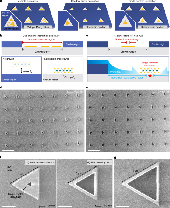
Nucleation control is fundamental to semiconductor deposition, governing when, where and how crystalline materials form. Conventional strategies can regulate nucleation density and, through area-selective growth, confine deposition to designated regions1,2,3,4,5,6,7,8,9,10,11,12,13. However, they generally do not determine where an individual nucleus forms within the growth regions, leaving even single-nucleation events spatially stochastic and limiting deterministic construction of crystalline materials. Here we report etching-flux-mediated single-centred nucleation of two-dimensional (2D) semiconductors to deterministically localize a single nucleation event. The etching flux released from the barrier suppresses nuclei near the pattern boundary, leaving a single surviving nucleus at the pattern centre, and systematic experiments elucidate the mechanism and establish nucleation design rules for zero, single and multiple nucleation regimes. Etching-flux-mediated single-centred nucleation enables single-crystal molybdenum disulfide growth at the 10-μm scale, field-effect mobilities of up to 117 cm2 V−1 s−1 and large-area uniformity with process compatibility. This in-plane chemical-flux strategy realizes spatially programmed growth, demonstrating nucleation–growth decoupling for line-shaped single crystals, multiple transistors integrated within a large common crystal, and aligned 2D lateral heterostructures for self-aligned contacts. These capabilities open a path towards advanced 2D electronic integration and expand semiconductor deposition from controlling where materials grow to controlling where and how crystals can begin to form.
Attaining highly localized and precise control of nucleation has emerged as a critical requirement in modern semiconductor processing, as such precision fundamentally governs uniformity and device performance. Area-selective growth (ASG) is a promising approach that deposits target materials on the desired regions, driven by a reaction-rate difference between growth and barrier regions. Over the past few decades, ASG has evolved through various approaches, including selective epitaxial growth of silicon–germanium stressors and III–V semiconductors1,2,3, selective metallization such as tungsten gap filling and cobalt capping4,5, and area-selective atomic layer deposition (AS-ALD) for oxide spacers and nitride barriers6,7. Recently, the ASG technique has been extended to two-dimensional (2D) transition-metal dichalcogenides (TMDs), which is a promising next-generation semiconductor, via selective chemical vapour deposition (CVD)8,9,10,11,12,13.
In 2D TMD ASG, selectivity can be realized by using heterogeneous surface patterning with a barrier region through mechanisms similar to those in three-dimensional (3D) bulk ASG processes. Recently, single-crystal 2D TMDs have been demonstrated through confined growth; however, the achievable crystal size remains limited8,9. As the entire growth region generally serves as a nucleation-active region (NAR) in conventional ASG, nucleation events occur stochastically at random sites within the growth region. Such stochastic nucleation behaviour constrains the attainable single-crystal domain size and hinders reliable spatial control, indicating the need for an advanced ASG strategy that enables large single-crystal growth and aligned heterostructure assembly.
To address these limitations, we developed an etching-flux-mediated single-centred nucleation (EF-SCN) strategy that introduces a paradigm for nucleation control in ASG systems. Unlike conventional 2D TMD ASG, which relies solely on out-of-plane selectivity through heterogeneous surface systems with different surface binding energies, EF-SCN achieves in-plane spatial control of nucleation by creating a non-uniform nucleation probability within the growth region. Oxygen released from an oxide barrier produces a lateral