// TOM'S HARDWARE US — HARDWARE & GADGET
China can make advanced chips without EUV, but the bill keeps growing
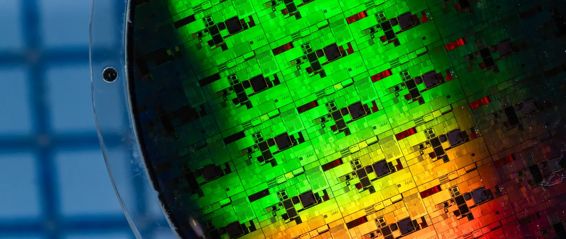
China has shown that older DUV lithography can be stretched much further than many expected – but can it fully catch up?
When you purchase through links on our site, we may earn an affiliate commission. Here’s how it works.
Export controls have kept ASML's most advanced EUV lithography machines out of China. Instead, the country's chipmaking industry has relied on less-capable deep ultraviolet (DUV) lithography machines. By using multiple exposures on critical chip layers, these older machines are still capable of producing performant silicon. However, as multiple patterns are applied there are more chances for defects, longer manufacturing times, and higher bills. We spoke to experts like Chris Mack, co-founder and CTO of semiconductor firm Fractilia, to find out how much further DUV can go.
For years, extreme ultraviolet (EUV) lithography has been seen as China’s biggest choke point in the country’s attempts to build cutting-edge chips. The machines, made exclusively by Dutch manufacturer ASML, use 13.5nm-wavelength light to print some of the most intricate features found on modern processors. Sales of ASML’s EUV systems are subject to export restrictions, forcing Chinese manufacturers to squeeze ever more out of older deep ultraviolet, or DUV, lithography instead. The EUV gap alone between China and the West is at least half a decade, according to some analysts.
But even without access to EUV machines, China has gotten surprisingly far in recreating what it offers through existing technology.
Teardowns of Huawei’s Mate 60 Pro in 2023 found the phone’s Kirin 9000S processor had been made by SMIC using a second-generation 7nm-class manufacturing process without EUV. More recently, analysis of Huawei’s Kirin 9030 found SMIC had pushed its DUV-based process closer still to the density associated with 5nm manufacturing – although it continued to lag behind the leading processes used by TSMC and Samsung.
The trick is multiple patterning. Rather than trying to print an overly intricate chip layer in a single pass, Chinese manufacturers are dividing up the complex design into several simpler patterns. Repeat the process enough times and you can etch up something approximating the proper layer you intended.
The trick works. But according to lithography expert Chris Mack, co-founder and CTO of Fractilia, asking whether a chip can be made without EUV overlooks the trade-offs manufacturers make in order to do it.
“When this transition first began, what everyone in the industry said as conventional wisdom is that cost-wise, three exposures on a 193 immersion tool cost about the same as one exposure on an EUV tool,” Mack said in an interview with Tom’s Hardware Premium. “At three, it was about even,” Mack explained. “But as soon as you hit four masks – 193 masks being replaced by one EUV mask – then EUV became more cost-effective.”
It’s also likely to produce a higher quality product with fewer defects. Each time a wafer is patterned, that new pattern has to line up perfectly with everything that’s already been etched beneath it. The more individual exposures needed to produce a single layer, the more opportunities there are for things to go wrong. “If you have, say, four 193 masks, you've got all those different overlays, and you've got all these different process variations that start to accumulate,” Mack said.